GET NEW INFO [Download 21+] Samsung G532 Schematic Diagram
Descargar Esquemático J2 Prime SM-G532M en PDF. TecnicoCell. Hola les traigo en esta ocasión el tan buscado plano esquemático y el manual del J2 Prime SM-G532F y SM-G532G para que puedas estudiarlo y resolver todas las fallas de micrófono, líneas dañadas del pin de carga, problemas en la memoria y más.

[Get 35+] Samsung G532 Schematic Diagram
Schematics . Attachments SM-G532G_Troubleshooting.pdf. File size 2 MB Views 0. SM-G532G_Product Specification.pdf. File size 3.8 MB Views 0. SM-G532G_Exploded View.pdf. File size 400.2 KB. Samsung Galaxy Grand Prime PRO SM-J250F Block Diagram. Admin; Jun 21, 2023; Schematics Phone & Tablet; Replies 0 Views 201. Jun 21, 2023. Admin. Samsung.
🛠 How to disassemble Samsung Galaxy J2 Prime SMG532 instruction
Daily Update 29 September 2020 . Complete Hardware Solution Samsung G532 . and SM-A207 - Galaxy A20s Service Manual + Xiaomi Mi A3 Schematics . GREAT.

[33+] Samsung G532f Schematic Diagram Download
Laptop hardware solutions. LAPTOP HARDWARE SOLUTIONS. acer. aspire 4738g (quanta zq9) aspire 4750 4750g 4752 je40 hr 10267. aspire 7471 je40 cp. aspire a111-31 quanta zge da0zhemb9e0. aspire a314-22 da0zhembc0 rev.c. aspire e1-410 ea40 bm mb 13233-1m.
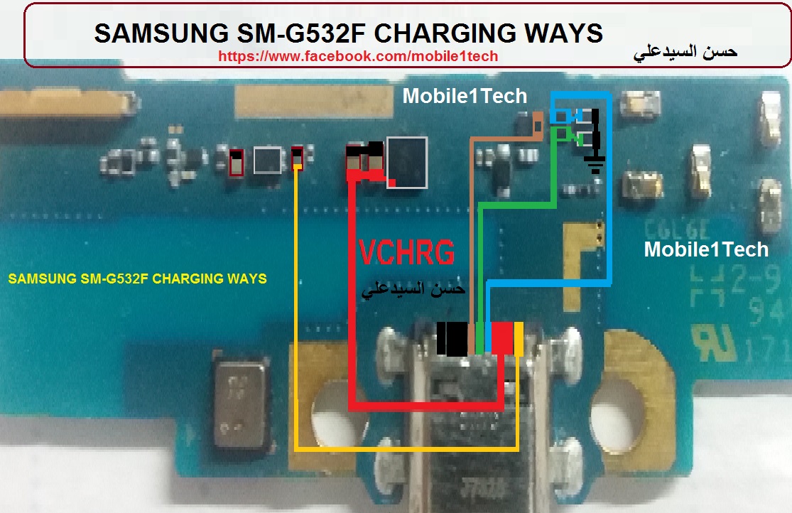
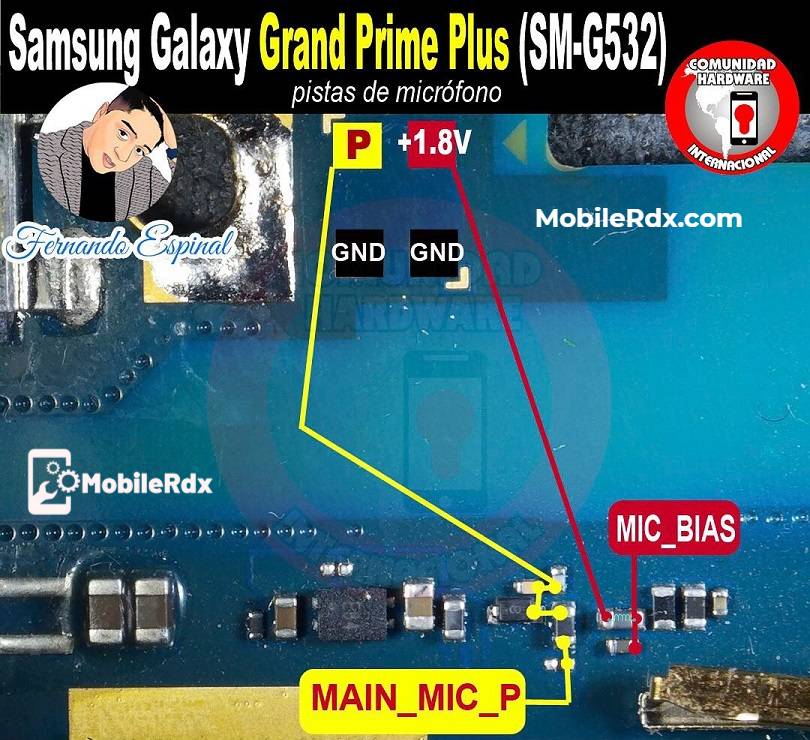
SAMSUNG SMG532F CHARGING WAYS
Samsung J2 Prime SM-G532G Schematics PCB Diagram | Easy FirmwareS 0 Home Packages & Pricing World Agents Contact Recent Files [ 2023-11-23 21:05:09 ] FEATURED [ 2023-11-23 21:01:59 ] FEATURED [ 2023-10-10 16:09:45 ] FEATURED [ 2023-10-10 16:08:45 ] [ 2023-10-10 16:07:37 ] [ 2023-10-10 16:06:53 ] [ 2023-10-10 16:06:22 ] [ 2023-10-10 16:05:18 ]
[Download 37+] Schematic Diagram Samsung G532g
Tải sơ đồ mạch mới nhất Samsung Galaxy J2 Prime SM-G532G schematics, tài liệu khắc phục sự cố và sửa chữa. Chi tiết mời anh em tải về ngay bên dưới đây. samsung J2 diagram. Reply. Axsam says: 2 years ago. Thank you. Reply. Leave a Reply Cancel reply. Your email address will not be published. Required.

sm g532 mic solution diagram YouTube
Mobile Phones Repairing and Technical Tips and Tricks *** *** *** SUBSCRIBE IFSA TECH.
agus [34+] Samsung G532f Schematic Diagram Download
Page 1 SM-G532F SM-G532F/DS SM-G532G/DS User Manual English. 10/2016. Rev.1.0 www.samsung.com. Page 2: Table Of Contents Messages SIM or USIM card Internet Memory card (microSD card) Email Turning the device on and off Camera Touchscreen Gallery Home screen Samsung Notes Lock screen Calendar Notification panel Voice Recorder Entering text My Files Screen capture Clock Opening apps.
[Get 35+] Samsung G532 Schematic Diagram
Schematics Phone & Tablet. SM-G532F Galaxy J2 Prime SCHEMATIC. Thread starter Admin; Start date Nov 26, 2018; Admin desktops & Laptops. Support. Nov 26, 2018 #1 SCHEMATIC SM-G532F SAMSUNG Galaxy J2 Prime . Attachments SM-G532F SVC Guide_Rev2.8.pdf. File size 3 MB Views 1. 08-SM-G532F_Tshoo_7.pdf.
[Get 35+] Samsung G532 Schematic Diagram
Page 1 User manual SM-G532G/DS.; Page 2 using this manual This user manual has been specially designed to guide you through the functions and features of your mobile phone. To get started quickly, refer to "introducing your mobile phone, Instructional icons Before you start, familiarise yourself with the icons you will see in this manual: Warning—situations that could cause injury to.

Samsung Galaxy Grand Prime Plus G532F Charging Problem Solution Jumper
Schematic samsung galaxy j2 prime sm-g532m sm-g532m-ds schematic. Thread starter Admin; Start date Jan 16, 2020; Tags samsung galaxy j2 prime sm-g532m sm-g532m-ds schematic Admin Founder. Staff member. Admin. Reputation: Jan 16, 2020 #1 samsung galaxy j2 prime sm-g532m sm-g532m-ds .
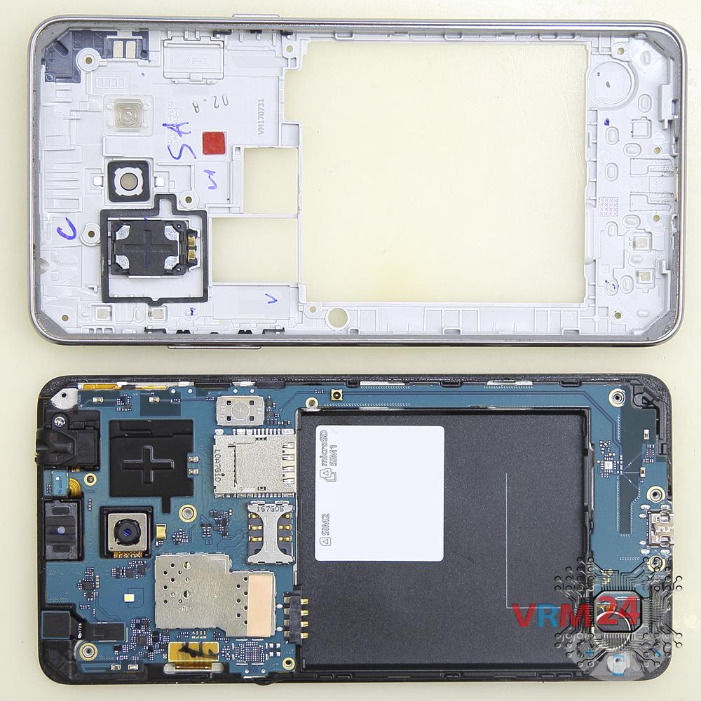
🛠 How to disassemble Samsung Galaxy J2 Prime SMG532 instruction
Reference SAMSUNG GALAXY J2 PRIME SM-G532G FRP RESET ADB MODE. kc gsm. Apr 28, 2022. Samsung. Reference Samsung Grand Prime (SM-G530W) Openline / Carrir. Alph1Tech. Jan 7, 2022. Samsung. Download Samsung All Mobile Schematics Diagram Here Free.
[Get 18+] Samsung G532f Schematic Diagram Download
Schematics Samsung schematics Nokia Xiaomi Schematics Rom Firmware Samsung Grand Prime Plus SM-G532F schematics Posted on September 18, 2020 By Admin Schematics Samsung Grand Prime Plus SM-G532F Download Samsung Grand Prime Plus SM-G532F schematics => Samsung Galaxy J2 Prime SM-G532G schematics Previous Post Xiaomi Redmi Note 7 schematics
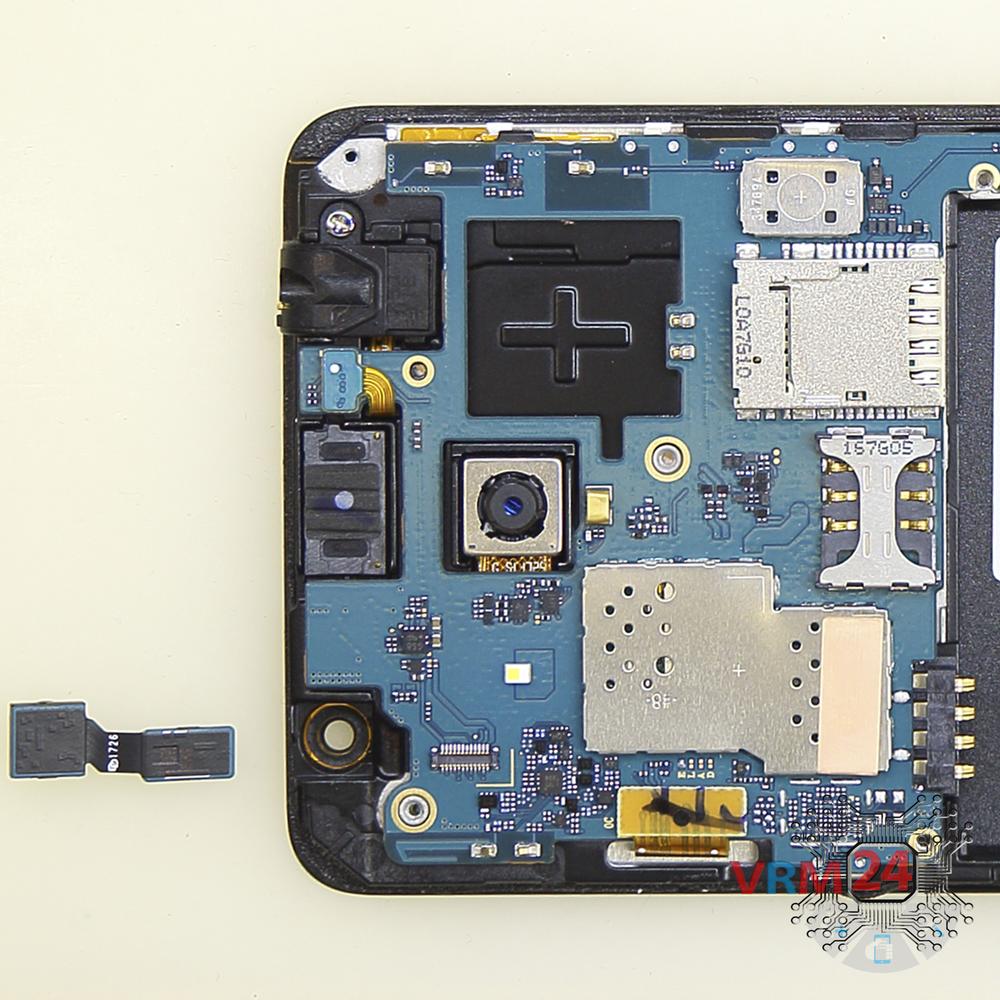
🛠 How to disassemble Samsung Galaxy J2 Prime SMG532 instruction
Display Back Light Fault Solution - First Time in youtube , Full details of Light IC,SM-G532G Light Ic In Details with Schematic Diagram,Samsung J2 Light Sol.
[35+] Samsung G532f Schematic Diagram Download
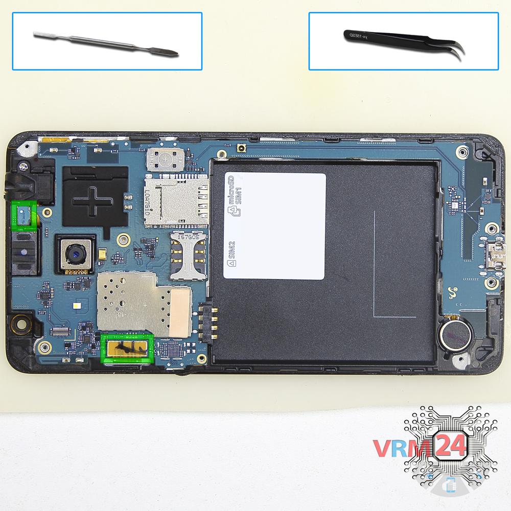
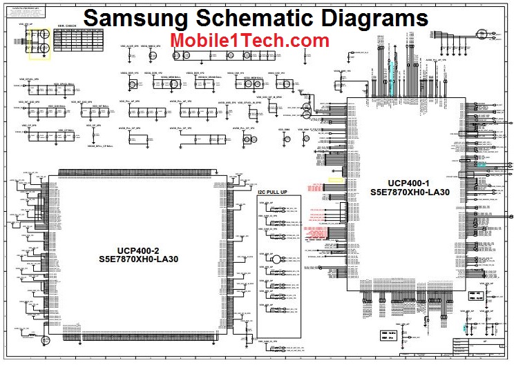
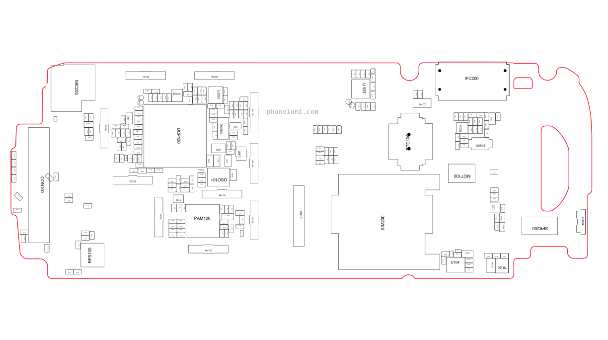
The schematic diagram for the Samsung G532g includes a detailed map of the phone's various components and their respective functions. This diagram is essential for anyone looking to repair, modify, or customize their device.
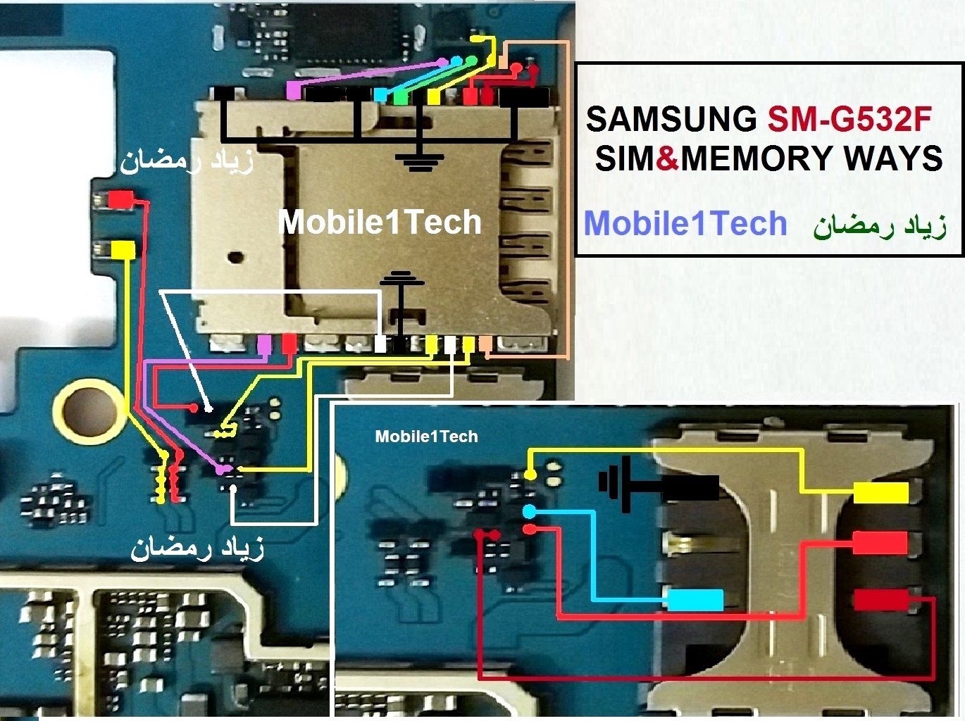
SAMSUNG SMG532F SIM&EMORY WAYS
Page 1 SM-G532F SM-G532F/DS SM-G532G/DS User Manual English. 10/2016. Rev.1.0 www.samsung.com f. Page 2 Table of Contents Basics Applications 4 Read me first 45 Installing or uninstalling apps 5 Package contents 47 Phone 6. Page 3 Table of Contents Settings 83 Introduction 83 Connections 92 Sounds and vibration 93 Notifications 93 Display 94.